


Het ontwerp van snelMulti-layer PCB-printplatenneeds to consider multiple aspects such as signal integrity, electromagnetic compatibility, and thermal management. Designers must accurately calculate the wire width, interlayer distance, and dielectric constant to ensure the stability and efficient transmission of the circuit. In addition, with the development of electronic devices towards miniaturization and high performance, higher requirements have been put forward for the number of layers and complexity of Multi-layer PCB-circuitplaten .
In ons productieproces omvat de snelle productie van Multi-Layer PCB-circuitboards geavanceerde fotolithografietechnologie, elektroplatingproces en laminatietechnologie . Elke stap vereist precieze controle om een nauwkeurige docking te waarborgen van elke laag van circuit en de algehele kwaliteit van het circuit van de circuit en het elektriciteit van de Coplating Process vereist Strikte controle van de Coplating Process om de dikte van de Coplating Process Strikte van de Coplating Process te waarborgen. Weerstand .
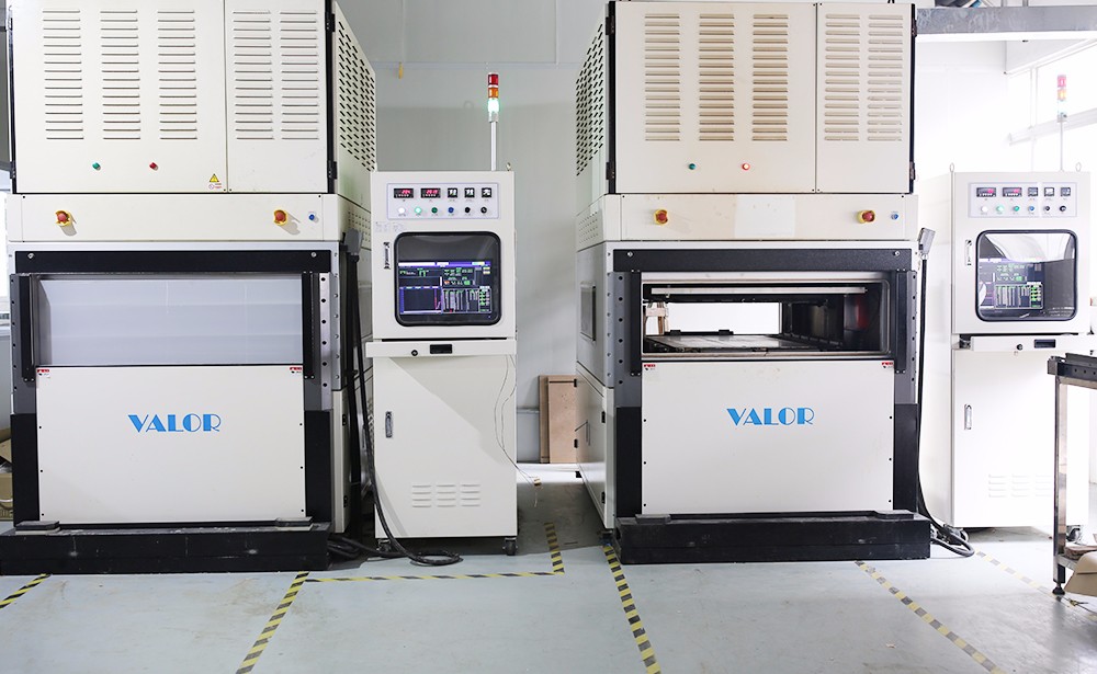
In terms of applications, fast multi-layer PCB circuit boards are widely used in fields such as communication equipment, computer systems, aerospace, medical equipment, etc. In these fields, circuit boards need to withstand high-frequency signal transmission, high current loads, and extreme temperature changes. Therefore, designing and manufacturing high-quality multi-layer PCB circuit boards is crucial for ensuring De stabiliteit van apparatuur en het verlengen van zijn servicevenstaat .
Om de prestaties van snelle Multi-Layer PCB-circuitplaten verder te verbeteren, onderzoeken we constant nieuwe materialen en processen ., bijvoorbeeld met behulp van materialen met lage diëlektrische constanten kan signaalvertraging verminderen, terwijl nieuwe thermische beheeroplossingen effectief warmte kunnen verspreiden en de betrouwbaarheid van het circuit kunnen verbeteren .}}}}}}}}}